
Notice that there is no audio artifact during the transitions between the two sine waves. Also the control signals can be seen here as a square pulse.
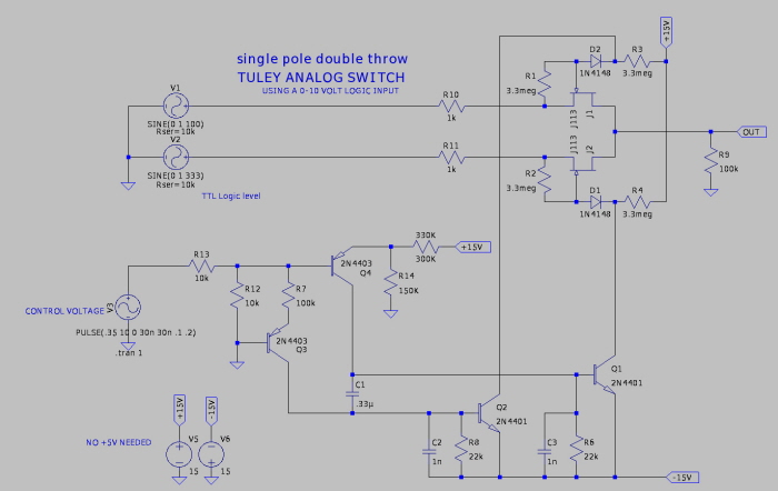
The 1st draft of the schematic which I will be breadboarding and debugging before committing this design to solder. There are no ic's, just discrete components.
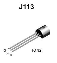
JFET leads reference will come in handy while building. Gate, Source, Drain.
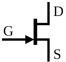
JFET cheat sheet which I will often refer to while I work.

PNP transistors used. Leads reference. Collector, Base, Emitter.


NPN transistors used. Leads reference. Collector, Base, Emitter.

Initial breadboard build and debug. I had to use 3 x .1 uf capacitors in parallel to come close enough to the .33 uf value in my spice model. Nice trick when exact value caps or resistors are not on hand.
Having some trouble with getting the A to B transition to occur. A Pspice simulation is an ideal case scenario. , Things can behave differently when actual components are utilized to realized the design. Looks like I need to revise the design a little more.

gLike
Fader - Module
While my original switch module meets my expectations for that design, I wanted to create a similar module which would operate a high frequencies without introducing any artifacts while transitioning between the two signals which are likely to be out of phase with one another. By replacing the switch mechanism in my previous design with that of an ultra fast crossfader mechanism the pop tick audio artifact is eliminated during A to B transitions.